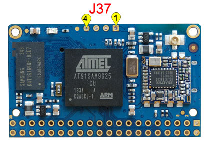
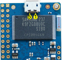
The follow sheet is for the WiFIG25 board, the linux inode row is for the linux.

| Pin # |
CPU pin |
Primary |
Description |
Alternate |
Description |
Alternate |
Description |
| 1 |
PB11 |
AD0 |
A/D input |
GPIO(43) |
General purpose I/O |
PWM0 |
Pulse Width Modulation |
| 2 |
PB12 |
AD1 |
A/D input |
GPIO(44) |
General purpose I/O |
PWM1 |
Pulse Width Modulation |
| 3 |
PB13 |
AD2 |
A/D input |
GPIO(45) |
General purpose I/O |
PWM2 |
Pulse Width Modulation |
| 4 |
PB14 |
AD3 |
A/D input |
GPIO(46) |
General purpose I/O |
PWM3 |
Pulse Width Modulation |
| 5 |
ADVREF |
ADVREF |
A/D voltage reference |
|
|
|
|
| 6 |
PA30 |
SDA0 |
I2C bus Data |
GPIO(30) |
General purpose I/O |
|
|
| 7 |
PA31 |
SCL0 |
I2C bus Clock |
GPIO(31) |
General purpose I/O |
|
|
| 8 |
PA0 |
TXD0 |
Serial TXD /dev/ttyS1 |
GPIO(0) |
General purpose I/O |
|
|
| 9 |
PA1 |
RXD0 |
Serial RXD /dev/ttyS1 |
GPIO(1) |
General purpose I/O |
|
|
| 10 |
PA2 |
RTS0 |
Serial RTS /dev/ttyS1 |
GPIO(2) |
General purpose I/O |
|
|
| 11 |
PA3 |
CTS0 |
Serial CTS /dev/ttyS1 |
GPIO(3) |
General purpose I/O |
|
|
| 12 |
PA4 |
GPIO |
General purpose I/O |
GPIO(4) |
|
|
|
| 13 |
PA5 |
TXD1 |
Serial TXD /dev/ttyS2 |
GPIO(5) |
General purpose I/O |
|
|
| 14 |
PA6 |
RXD1 |
Serial RXD /dev/ttyS2 |
GPIO(6) |
General purpose I/O |
|
|
| 15 |
PA7 |
TXD2 |
Serial TXD /dev/ttyS3 |
GPIO(7) |
General purpose I/O |
|
|
| 16 |
PA8 |
RXD2 |
Serial RXD /dev/ttyS3 |
GPIO(8) |
General purpose I/O |
|
|
| 17 |
PA12 |
MOSI |
SPI MOSI |
GPIO(12) |
General purpose I/O |
|
|
| 18 |
PA11 |
MISO |
SPI MISO |
GPIO(11) |
General purpose I/O |
|
|
| 19 |
PA13 |
SPCK |
SPI CLOCK |
GPIO(13) |
General purpose I/O |
|
|
| 20 |
PA14 |
NPCS0 |
SPI CS0 |
GPIO(14) |
General purpose I/O |
|
|
| 21 |
GND |
|
Ground line |
|
|
|
|
| 22 |
PB3 |
1W |
Bit banging 1-wire bus |
SPI CS3 |
SPI CS3 |
GPIO(35) |
General purpose I/O |
| 23 |
USBCP |
D+ |
USB 2.0 Host full-speed port C |
|
|
|
|
| 24 |
USBCN |
D- |
USB 2.0 Host full-speed port C |
|
|
|
|
| 25 |
PC27 |
RTS1 |
Serial RTS /dev/ttyS2 |
GPIO(91) |
General purpose I/O |
|
|
| 26 |
PB0 |
RTS2 |
Serial RTS /dev/ttyS3 |
GPIO(32) |
General purpose I/O |
|
|
| 27 |
USBAN |
D- |
USB 2.0 Host/Device hi-speed port A |
|
|
|
|
| 28 |
USBAP |
D+ |
USB 2.0 Host/Device hi-speed port A |
|
|
|
|
| 29 |
PC18 |
PWM0 |
Pulse Width Modulation |
GPIO(82) |
General purpose I/O |
|
|
| 30 |
PC19 |
PWM1 |
Pulse Width Modulation |
GPIO(83) |
General purpose I/O |
|
|
| 31 |
PC20 |
PWM2 |
Pulse Width Modulation |
GPIO(84) |
General purpose I/O |
|
|
| 32 |
PC21 |
PWM3 |
Pulse Width Modulation |
GPIO(85) |
General purpose I/O |
|
|
| 33 |
PC2 |
TIOA3 |
TC block PWM0 |
GPIO(66) |
General purpose I/O |
|
|
| 34 |
PC3 |
TIOB3 |
TC block PWM1 |
GPIO(67) |
General purpose I/O |
|
|
| 35 |
PC4 |
TCLK3 |
TC block CLOCK |
GPIO(68) |
General purpose I/O |
|
|
| 36 |
VDD5V |
|
5V0 power in/out |
|
|
|
|
| 37 |
VDD33 |
|
3V3 power out |
|
|
|
|
| 38 |
GND |
|
Ground line |
|
|
|
|
| 39 |
VBAT |
VBAT |
RTC battery in |
|
|
|
|
| 40 |
NRST |
NRST |
Reset input/output signal (active low) |
|
|
|
|

| Pin # |
CPU Pin |
Primary |
Description |
|
|
|
| 1 |
VDD5V |
|
5V0 power in/out |
|
|
|
| 2 |
PA9 |
DRXD |
Debug serial port |
|
|
|
| 3 |
PA10 |
DTXD |
Debug serial port |
|
|
|
| 4 |
GND |
|
Ground line |
|
|
|
|

| Pin # |
CPU Pin |
Primary |
Description |
|
|
|
| 1 |
VDD5V |
|
5V0 power in |
|
|
|
| 2 |
USBAN |
|
Data- |
|
|
|
| 3 |
USBAP |
|
Data+ |
|
|
|
| 4 |
ID |
|
|
|
|
|
| 5 |
GND |
|
Ground line |
|
|
|
|


 微博
微博
