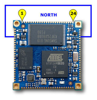
• The follow sheet is for the CORE9X35 board, the 2.6x and 3.1x row is only for the debian system. 
Pin # IC Pin Default Alt 2.6x 3.1x Note
N1   3V3       Power In Vcc
N2 PC0 GPIO SDA1 96 64 I2C bus 1 Data or GPIO
N3 PC1 GPIO SCL1 97 65 I2C bus 1 Clock or GPIO
N4 PC2 B2 GPIO     LCD Blue B2
N5 PC3 B3 GPIO     LCD Blue B3
N6 PC4 B4 GPIO     LCD Blue B4
N7 PC5 B5 GPIO     LCD Blue B5
N8 PC6 B6 GPIO     LCD Blue B6
N9 PC7 B7 GPIO     LCD Blue B7
N10 PC8 GPIO UTXD0 104 72  
N11 PC9 GPIO URXD0 105 73  
N12 PC10 G2 GPIO     LCD Green G2
N13 PC11 G3 GPIO     LCD Green G3
N14 PC12 G4 GPIO     LCD Green G4
N15 PC13 G5 GPIO     LCD Green G5
N16 PC14 G6 GPIO     LCD Green G6
N17 PC15 G7 GPIO     LCD Green G7
N18 PC16 GPIO UTXD1 112 80  
N19 PC17 GPIO URXD1 113 81  
N20 PC18 R2 GPIO     LCD Red R2
N21 PC19 R3 GPIO     LCD Red R3
N22 PC20 R4 GPIO     LCD Red R4
N23 PC21 R5 GPIO     LCD Red R5
N24   GND       Power In GND
Pin # IC Pin Default Alt ID 2.6x ID 3.1x Note
E1   GND       Power In Vcc
E2 PC22 R6 GPIO     LCD Red R6
E3 PC23 R7 GPIO     LCD Red R7
E4 PC24 LCDDISP GPIO     LCD signal
E5 PC25   GPIO     LCD signal
E6 PC26 LCDPWM       LCD signal
E7 PC27 VSYNC GPIO     LCD signal
E8 PC28 HSYNC GPIO     LCD signal
E9 PC29 LCDDEN       LCD signal
E10 PC30 LCDPCK       LCD signal
E11 PC31 GPIO   127 95  
E12 USBCP D+       USB 2.0 Host full-speed port C
E13 USBCN D-       USB 2.0 Host full-speed port C
E14   GND       Power In GND
E15 USBBN D-       USB 2.0 Host hi-speed port B
E16 USBBP D+       USB 2.0 Host hi-speed port B
E17   GND       Power In GND
E18 USBAN D-       USB 2.0 Host/Device hi-speed port A
E19 USBAP D+       USB 2.0 Host/Device hi-speed port A
E20 VBAT         RTC battery backup +3 volt DC input
E21 NRST         Reset input signal (active low)
E22 SHDN         Shutdown output signal (active low)
E23 WKUP         Wake-up input signal (active low)
E24   3V3       Power In Vcc
Pin # IC Pin Default Alt ID 2.6x ID 3.1x Note
S1   3V3       Power In Vcc
S2 PA21 1W GPIO 53 21 Bit banging 1-wire bus or GPIO
S3 PA20 DA3   52 20 microSD Card memory
S4 PA19 DA2   51 19 microSD Card memory
S5 PA18 DA1   50 18 microSD Card memory
S6 PA17 CK   49 17 microSD Card memory
S7 PA16 CDA   48 16 microSD Card memory
S8 PA15 DA0   47 15 microSD Card memory
S9 PA14 NPCS0 GPIO 46 14 SPI bus 0 chip select 0 or GPIO
S10 PA13 SPCK GPIO 45 13 SPI bus 0 clock or GPIO
S11 PA12 MOSI GPIO 44 12 SPI bus 0 Master Output or GPIO
S12 PA11 MISO GPIO 43 11 SPI bus 0 Master Input or GPIO
S13 PA10 DTXD   42 10 Debug serial port
S14 PA9 DRXD   41 9 Debug serial port
S15 PA8 RXD2 GPIO 40 8 Serial line /dev/ttyS3 RXD or GPIO
S16 PA7 TXD2 GPIO 39 7 Serial line /dev/ttyS3 TXD or GPIO
S17 PA6 CANRX1 RXD1 38 6 CAN bus or Serial line
S18 PA5 CANTX1 TXD1 37 5 CAN bus or Serial line
S19 PA4 GPIO   36 4  
S20 PA3 CTS0 GPIO 35 3 Serial line /dev/ttyS1 CTS or GPIO
S21 PA2 RTS0 GPIO 34 2 Serial line /dev/ttyS1 RTS or GPIO
S22 PA1 RXD0 GPIO 33 1 Serial line /dev/ttyS1 RXD or GPIO
S23 PA0 TXD0 GPIO 32 0 Serial line /dev/ttyS1 TXD or GPIO
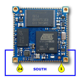
S24   GND       Power In GND
Pin # IC Pin Default Alt ID 2.6x ID 3.1x Note
W1   GND       Power In GND
W2   ETHRXP       Eth RX+
W3   ETHRXN       Eth RX-
W4   ETHTXP       Eth TX+
W5   ETHTXN       Eth TX-
W6   ETH3V3       Eth 3V3
W7   ETHLED1       Eth Yellow led (traffic)
W8   ETHLED2       Eth Green led (link)
W9 PA22 GPIO   54 22  
W10 PA23 GPIO   55 23  
W11 PA24 GPIO   56 24  
W12 PA25 GPIO   57 25  
W13 PA26 GPIO   58 26  
W14 PA27 GPIO   59 27  
W15 PA28 GPIO   60 28  
W16 PA29 GPIO   61 29  
W17 PA30 SDA0 GPIO 62 30 I2C bus 0 Data or GPIO
W18 PA31 SCL0 GPIO 63 31 I2C bus 0 Clock or GPIO
W19 ADVREF         A/D converter voltage reference In (max 3.3 volt)
W20 PB11 X+ GPIO 75 43 Touchsreen X+
W21 PB12 X- GPIO 76 44 Touchsreen X-
W22 PB13 Y+ GPIO 77 45 Touchsreen Y+
W23 PB14 Y- GPIO 78 46 Touchsreen Y-
W24   3V3       Power In Vcc
关注我们: 微博

销售邮箱:market@armdevs.com
技术支持: support@armdevs.com
销售电话: +86-755-29638421


核风在线支持>
在线时间:09:00-18:00
Copyright @ 2014 to 2020 - 核风智能技术有限公司